

SiC Wafer Polishing Market Revenue to Rise from US$ 850.0 Million in 2025 to US$ 5,950.1 Million by 2033
The global semiconductor manufacturing landscape is experiencing a profound structural transition, heavily influenced by an accelerating reliance on wide-bandgap substrates over conventional silicon to withstand the high-power workloads and severe thermal constraints of next-generation applications.
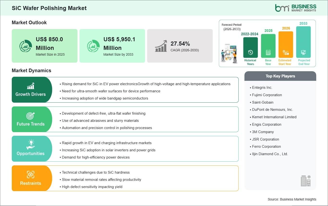
Business Market Insights forecasts that the global SiC Wafer Polishing Market value will surge to US$ 5,950.1 million by 2033 from its 2025 baseline of US$ 850.0 million, progressing at a robust CAGR of 27.54% over the 2026–2033 forecast period.
Recent shifts toward 800V automotive architectures and ultra-fast EV charging networks are fundamentally altering market dynamics. Leading semiconductor equipment and consumable manufacturers are aggressively developing advanced diamond slurries and next-generation Chemical-Mechanical Polishing (CMP) systems to significantly increase material removal rates (MRR) while drastically reducing the time and cost associated with processing these ultra-hard substrates.
Download Sample Report : https://www.businessmarketinsights.com/sample/BMIPUB00034334
What Is SiC Wafer Polishing?
SiC wafer polishing is the critical final step in the preparation of silicon carbide substrates before epitaxial growth and microchip fabrication can occur. Silicon carbide is one of the hardest synthetic materials on earth, ranking just below diamond on the Mohs scale. Slicing SiC ingots into raw wafers leaves severe microscopic surface damage, scratches, and saw marks that would immediately cause advanced electronic circuits to fail.
The polishing process utilizes specialized equipment to apply highly engineered abrasive slurries—typically containing synthetic diamond particles or colloidal silica—and polyurethane polishing pads. Through a combination of mechanical abrasion and chemical reactions (Chemical-Mechanical Polishing, or CMP), the process aggressively removes the damaged surface layers and achieves an atomically smooth, mirror-like finish with surface roughness measured in sub-nanometers.
Market Drivers
The primary driver accelerating the SiC Wafer Polishing Market is the exponential growth of the global Electric Vehicle (EV) industry. Automakers are rapidly shifting from 400V to 800V battery architectures to reduce charging times and increase vehicle range. SiC-based power inverters operate at much higher temperatures and voltages with significantly less energy loss compared to traditional silicon. This creates a massive, sustained demand for high-quality SiC wafers, directly driving the need for scalable, high-yield polishing solutions.
Furthermore, the global push for renewable energy integration and smart grid infrastructure acts as a powerful market catalyst. High-power solar inverters and wind turbine power conversion systems heavily rely on SiC MOSFETs to maximize power transmission efficiency. As global installations of clean energy grids surge, the volume of SiC devices required—and consequently the volume of wafers needing precision polishing—is multiplying exponentially.
Additionally, the transition from 6-inch (150mm) to 8-inch (200mm) SiC wafers is heavily influencing market demand. While 8-inch wafers significantly lower the cost per chip, their larger surface area exponentially increases the difficulty of maintaining absolute planarization (flatness) across the entire wafer. This transition is forcing semiconductor foundries to completely overhaul their polishing lines, driving massive capital investments into state-of-the-art CMP machinery and advanced consumable slurries.
Market Segmentation
By Product Type
- Diamond Slurries
- Polishing Pads
- Colloidal Silica Suspensions
- Abrasive Powders
- Others
By Process
- Chemical-Mechanical Polishing (CMP)
- Mechanical Polishing
- Plasma-Assisted Polishing
- Electropolishing
By Wafer Size
- 4-Inch and Below
- 6-Inch (150mm)
- 8-Inch (200mm)
By Application
- Power Electronics
- Light-Emitting Diodes (LEDs)
- RF & Microwave Devices
- Sensors & Detectors
The Diamond Slurries segment commands the highest market share in terms of consumables, due to the absolute necessity of using ultra-hard abrasives to effectively cut and smooth the SiC surface. However, the Chemical-Mechanical Polishing (CMP) segment dominates the process category, as pure mechanical polishing often leaves residual subsurface damage. By wafer size, the 6-inch segment currently drives the majority of production volume, while the 8-inch segment is projected to exhibit the fastest growth rate as top-tier foundries rapidly commercialize larger formats. Power Electronics stands as the undisputed leading application, directly fueled by EV and industrial inverter demand.
Regional Insights
- Asia-Pacific commands the largest global market share and is the epicenter of semiconductor manufacturing. This absolute dominance is driven by immense domestic EV production in China, alongside massive, state-backed investments in wide-bandgap semiconductor foundries across Taiwan, Japan, and South Korea. The region's dense concentration of wafer manufacturers creates an unparalleled demand for polishing equipment and high-grade consumables.
- North America holds a highly strategic and rapidly expanding market position. Growth is propelled by aggressive government initiatives, such as the US CHIPS and Science Act, which provides billions in funding to onshore critical semiconductor manufacturing. The region is home to several dominant SiC wafer producers, driving intense localized demand for advanced polishing solutions to secure domestic EV supply chains.
- Europe maintains a robust market position anchored by its premium automotive engineering sector. European automakers and tier-one suppliers are actively securing long-term SiC wafer supplies to meet the European Union's stringent internal combustion engine phase-out mandates. This is fueling massive regional investments into new SiC fabrication plants, directly boosting the polishing equipment market.
- Middle East & Africa and South America are currently in emerging stages of adoption. As GCC nations diversify their economies into high-tech manufacturing and renewable energy infrastructure, the foundational groundwork for specialized semiconductor component assembly—and eventually localized wafer processing—is gradually being laid.
Top Players in the SiC Wafer Polishing Industry
The competitive landscape is characterized by a high barrier to entry, heavily reliant on complex material science and precision engineering. The market is led by specialized slurry chemical formulators and advanced CMP machinery manufacturers.
- Applied Materials, Inc.
- Revasum, Inc.
- Entegris, Inc.
- DuPont de Nemours, Inc.
- 3M Company
- Engis Corporation
- JSR Corporation
- Saint-Gobain
- EBARA Corporation
- Kemet International Ltd.
To capture market share, these tier-one providers are continuously investing in R&D to develop "slurry-pad" synergy systems—highly optimized combinations of chemical suspensions and engineered polishing pads designed specifically to maximize material removal rates on SiC while minimizing expensive consumable waste.
Technological Innovations
Technological innovations in Plasma-Assisted Polishing (PAP) are pushing the boundaries of SiC surface finishing. Traditional CMP struggles with the extreme chemical inertness and hardness of SiC, resulting in painfully slow processing times. PAP uses atmospheric-pressure plasma to irradiate the SiC wafer surface, modifying the top atomic layers into a softer oxide film. This softened layer is then easily removed using mild, abrasive-free polishing pads. This breakthrough drastically reduces the need for expensive diamond slurries, eliminates subsurface mechanical damage, and significantly accelerates the overall polishing cycle.
Furthermore, the development of Automated Double-Sided Polishing (DSP) systems is revolutionizing mass production. Next-generation DSP machinery allows both sides of the SiC wafer to be polished simultaneously with perfect planarization control. Integrated with closed-loop AI thickness sensors, these machines can automatically adjust polishing pressure across different zones of the pad in real-time, completely eliminating the human error associated with traditional batch polishing and ensuring maximum wafer yield.
Future Market Outlook
The long-term trajectory for the SiC Wafer Polishing Market is heavily tied to the ultimate transition toward 8-inch (200mm) SiC wafers. As the industry scales to 8-inch, the available area per wafer nearly doubles, which will crash the cost of SiC power chips and accelerate their adoption beyond premium EVs into mid-range consumer vehicles and mainstream industrial motors.
Moving forward, the industry will see a heightened focus on slurry recycling and circular manufacturing. Because diamond slurries and specialized colloidal silica are exceptionally expensive and environmentally taxing to dispose of, the next frontier of market competition will revolve around inline slurry filtration and recovery systems. Manufacturers who can offer high-performance polishing processes coupled with closed-loop chemical recycling will capture the highest premium contracts in an increasingly eco-conscious semiconductor landscape.
Frequently Asked Questions (FAQs)
Why is polishing Silicon Carbide (SiC) more difficult than standard Silicon?
Silicon carbide is incredibly hard—approaching the hardness of a diamond—and highly chemically inert. While standard silicon can be quickly polished using mild chemicals and soft silica pads, SiC requires extremely aggressive diamond abrasives, higher mechanical pressure, and specialized chemical catalysts, making the process much longer, more expensive, and technically complex.
What is Chemical-Mechanical Polishing (CMP) in the context of SiC?
CMP is a hybrid process. The chemical component in the slurry softens or oxidizes the absolute top atomic layer of the SiC wafer, while the mechanical component (the abrasive particles and the polishing pad) sweeps that softened layer away. This alternating reaction ensures the surface becomes perfectly flat without inflicting deep microscopic cracks.
Why is the transition from 6-inch to 8-inch SiC wafers important for the polishing market?
An 8-inch wafer yields roughly 80% more usable chips than a 6-inch wafer, which will drastically lower the cost of SiC power electronics. However, polishing a larger surface while maintaining absolute flatness across the entire diameter is exponentially harder. This forces manufacturers to buy entirely new, state-of-the-art polishing equipment and highly specific consumables, driving massive market revenue.
What role do diamond slurries play in SiC polishing?
Because SiC is so hard, standard abrasives wear down too quickly or fail to cut the material. Diamond slurries contain microscopic, synthetic diamond particles suspended in a chemical fluid. These particles are hard enough to physically sheer away the rough peaks of the SiC wafer, making them the most critical—and expensive—consumable in the mechanical polishing phase.
Browse More Reports:
https://www.businessmarketinsights.com/reports/steel-casting-market
https://www.businessmarketinsights.com/reports/street-and-roadway-lighting-market
https://www.businessmarketinsights.com/reports/structural-foam-market
About Us
Business Market Insights is a market research platform that provides a comprehensive subscription service for targeted industry and company intelligence reports. Our research team has extensive professional expertise across dynamic industrial domains such as Electronics & Semiconductor; Aerospace & Defense; Automotive & Transportation; Energy & Power; Healthcare; Manufacturing & Construction; Food & Beverages; Chemicals & Materials; and Technology, Media, & Telecommunications.
Contact Us
If you have any questions about this report or would like further information, please contact us:
Contact person: Ankit Mathur
Email: sales@businessmarketinsights.com
Phone: +16467917070