

Japan Semiconductor Foundry Market Size, Growth, Trends and Demand Report 2026–2034
Japan Semiconductor Foundry Market Report 2026
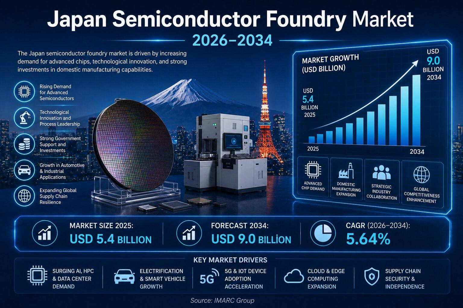
Market Size in 2025: USD 5.4 Billion
Market Forecast in 2034: USD 9.0 Billion
Market Growth Rate: 5.64% (2026–2034)
According to the latest report by IMARC Group, titled "Japan Semiconductor Foundry Market: Industry Trends, Share, Size, Growth, Opportunity and Forecast 2026-2034," the Japan Semiconductor Foundry market size reached USD 5.4 Billion in 2025. Looking forward, IMARC Group expects the market to reach USD 9.0 Billion by 2034, exhibiting a growth rate (CAGR) of 5.64% during 2026-2034.
Request PDF Sample for more detailed market insights: https://www.imarcgroup.com/japan-semiconductor-foundry-market/requestsample
Japan Semiconductor Foundry Industry Trends and Demands in 2026:
Japan's semiconductor foundry market is experiencing robust growth driven by government strategic investment in domestic semiconductor manufacturing capacity rebuilding through the METI semiconductor strategy and RAPIDUS advanced node foundry development program, increasing geopolitical supply chain security motivation driving Japanese OEMs and system companies to seek domestic and allied-nation semiconductor sourcing alternatives to Taiwan and China concentration, growing automotive semiconductor demand from Japan's vehicle electrification transition requiring power semiconductor and automotive-grade microcontroller supply security, expanding TSMC Kumamoto facility production serving Japanese automotive and industrial semiconductor customers, and rising demand for compound semiconductor and power device foundry capacity serving EV and renewable energy application markets. The market covers 10/7/5nm, 16/14nm, 20nm, 45/40nm, and other technology node segments. Foundry type segments include pure play foundry and integrated device manufacturer (IDM) models. Application segments span communication, consumer electronics, computer, automotive, and others. Japan's RAPIDUS 2nm node foundry program targeting 2027 pilot production represents the most strategically significant domestic advanced semiconductor manufacturing initiative since Japan's 1980s technology leadership era. TSMC's Kumamoto Fab 1 producing 12/16nm node process for Sony, Denso, and other Japanese customers marks the first major new semiconductor manufacturing facility opening in Japan in decades. Automotive semiconductor demand is the highest-growth application driven by Japan's vehicle electrification transition creating unprecedented power semiconductor and automotive microcontroller supply requirements. Power semiconductor foundry capacity for silicon carbide and gallium nitride devices is growing alongside EV drivetrain and charging infrastructure application demand. Mature node foundry capacity for analog, mixed-signal, and power management applications serving industrial and automotive customers is sustaining stable revenue through the forecast period.
The market reflects Japan's semiconductor industry strategic revival after decades of relative decline, driven by government recognition of semiconductor supply chain security as a national economic and defense priority. Pure play foundry capacity is expanding through TSMC Kumamoto operations and emerging domestic foundry investment alongside IDM manufacturers including Renesas, Toshiba, and Rohm maintaining captive and open foundry capacity for specialty process technologies. Advanced node development through RAPIDUS is targeting high-performance computing, AI accelerator, and next-generation communication chip applications for domestic and international fabless semiconductor customers. Japanese fabless and IDM semiconductor companies are evaluating domestic foundry sourcing for supply chain security risk reduction even where cost premiums apply relative to Taiwan alternatives. Research institute partnership with IMEC and international semiconductor research consortia is supporting RAPIDUS technology development capability building for advanced node process integration.
How AI is Reshaping the Future of the Japan Semiconductor Foundry Market:
AI-Powered Process Control and Yield Optimization:
AI analyzes real-time semiconductor fabrication process sensor data including thin film deposition rate, etch rate uniformity, photolithography overlay accuracy, and defect inspection scan results to identify process parameter drift patterns and automatically adjust equipment control setpoints maintaining process window centering and improving wafer yield across advanced and mature node production lines. Machine learning models trained on historical process condition and yield outcome datasets improve defect root cause identification accuracy and process optimization recommendation quality. These capabilities are critical enablers for Japan's RAPIDUS advanced node ambition where process window control at sub-5nm dimensions requires AI-assisted automated process control sophistication beyond conventional statistical process control methodology capability.
Predictive Equipment Maintenance and Fab Productivity:
AI monitors semiconductor fabrication equipment performance parameters including chamber condition indicators, consumable wear state, vacuum system performance, and process gas purity to predict maintenance requirements and unscheduled downtime events before wafer production disruption occurs. Machine learning models analyze multi-tool process data correlation patterns identifying systemic equipment condition deterioration impacting multiple process steps enabling coordinated preventive maintenance scheduling minimizing fab capacity loss impact. These technologies maximize semiconductor foundry equipment utilization efficiency, reduce unplanned production disruption costs, and support Japan's foundry operators in delivering competitive fab productivity metrics required for international fabless customer qualification and ongoing supply commitments.
AI-Driven Chip Design Enablement and Design-Technology Co-Optimization:
AI analyzes semiconductor device physics simulation data, process design kit parameter libraries, and circuit performance characterization datasets to generate optimized standard cell libraries, physical design rule recommendations, and design-for-manufacturability guideline improvements enabling fabless customer chip designs to achieve superior yield and performance outcomes at Japan's foundry process nodes. Machine learning models identify layout pattern combinations with elevated systematic defect risk enabling design rule check enhancement and automated layout optimization tool development. These capabilities support Japan's foundry operators in providing superior design enablement service value to domestic and international fabless semiconductor customers, accelerate customer design-to-production timelines through more accurate first-silicon performance prediction, and differentiate Japan's foundry technology offering through AI-enhanced process-design co-optimization partnership programs.
Japan Semiconductor Foundry Market Segmentation:
The market report offers a comprehensive analysis of the segments, highlighting those with the largest Japan Semiconductor Foundry market share. It includes forecasts for the period 2026-2034 and historical data from 2020-2025 for the following segments.
Technology Node Insights:
- 10/7/5nm
- 16/14nm
- 20nm
- 45/40nm
- Others
Foundry Type Insights:
- Pure Play Foundry
- Integrated Device Manufacturers (IDMs)
Application Insights:
- Communication
- Consumer Electronics
- Computer
- Automotive
- Others
Regional Insights:
- Kanto Region
- Kansai/Kinki Region
- Central/Chubu Region
- Kyushu-Okinawa Region
- Tohoku Region
- Chugoku Region
- Hokkaido Region
- Shikoku Region
Competitive Landscape:
The report offers an in-depth examination of the competitive landscape encompassing market structure, key player positioning, leading strategies for success, a competitive dashboard, and a company evaluation quadrant. Additionally, the report features detailed profiles of all major companies in the Japan Semiconductor Foundry industry.
- RAPIDUS Corporation
- Taiwan Semiconductor Manufacturing Company (TSMC Kumamoto)
- Renesas Electronics Corporation
- Rohm Semiconductor
- Toshiba Electronic Devices & Storage Corporation
- Sony Semiconductor Solutions Corporation
Recent News and Developments in Japan Semiconductor Foundry Market
April 2026: RAPIDUS Corporation announced advancement of its 2nm node process development program at its Chitose, Hokkaido facility with IBM research partnership milestones achieved, targeting pilot production capability demonstration by 2027 ahead of planned commercial production serving high-performance computing, AI accelerator, and next-generation mobile communication chip fabless customer engagements.
March 2026: TSMC Kumamoto Fab 1 reported strong production ramp progress serving Sony Semiconductor, Denso, and other initial Japanese automotive and imaging sensor customers, with Fab 2 advanced node construction approval announced targeting expanded domestic Japanese semiconductor supply capacity serving Japan's automotive electrification and advanced image sensing technology requirements.
Ongoing: Increasing investments in RAPIDUS 2nm node process development, TSMC Kumamoto Fab 2 advanced node capacity expansion, automotive semiconductor power device foundry capacity growth, silicon carbide and gallium nitride compound semiconductor foundry development, AI-powered yield optimization and process control capability deployment, government semiconductor manufacturing strategic subsidy program execution, and fabless customer design enablement service enhancement continue to reshape the Japan Semiconductor Foundry market.
Note: If you need specific information that is not currently within the scope of the report, we will provide it to you as a part of the customization.
About Us:
IMARC Group is a global management consulting firm that helps the world's most ambitious changemakers to create a lasting impact. The company provides a comprehensive suite of market entry and expansion services including thorough market assessment, feasibility studies, company incorporation assistance, factory setup support, regulatory approvals and licensing navigation, branding, marketing and sales strategies, competitive landscape and benchmarking analyses, pricing and cost research, and procurement research.
Contact Us:
Street: 563-13 Kamien
Area: Iwata
Country: Tokyo, Japan
Postal Code: 4380111
Email: sales@imarcgroup.com